Shisong attended DRC 2024 in University of Maryland with two papers! Congratulations! 1. S. Luo, C. Chang, Q. Xie, T. Li, M. Xu, Z. He, T. Palacios, and Y. Zhao, “GaN E-mode Complementary Transistors Based[…]
Category: Publication
Turning Up the Heat on Next-Generation Semiconductors!
Our collaboration paper with MIT and OSU is highlighted in MIT News and other media outlets. https://news.mit.edu/2024/turning-up-heat-on-next-generation-semiconductors-0523 High temperature stability of regrown and alloyed Ohmic contacts to AlGaN/GaN heterostructure up to 500 °C Appl. Phys.[…]
Mingfei’s Paper on h-BN/c-BN Published in APL!!
In this work, we synthesized mixed-phase hexagonal-boron nitride (h-BN)/cubic-BN (c-BN) composites with varying ratios and investigated their frequency and temperature-dependent dielectric properties. As the ratio of c-BN increased, we observed a corresponding increase in the[…]
UWBG Review Paper published in Oxford Open Materials Science
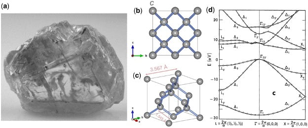
We published an invited review paper in the Oxford Open Materials Science! Please go to the publication website for details. Ultrawide bandgap (UWBG) materials such as diamond, Ga2O3, hexagonal boron nitride (h-BN) and AlN, are[…]
Kai’s Paper on GaN Selective Area Regrowth Accepted in APL
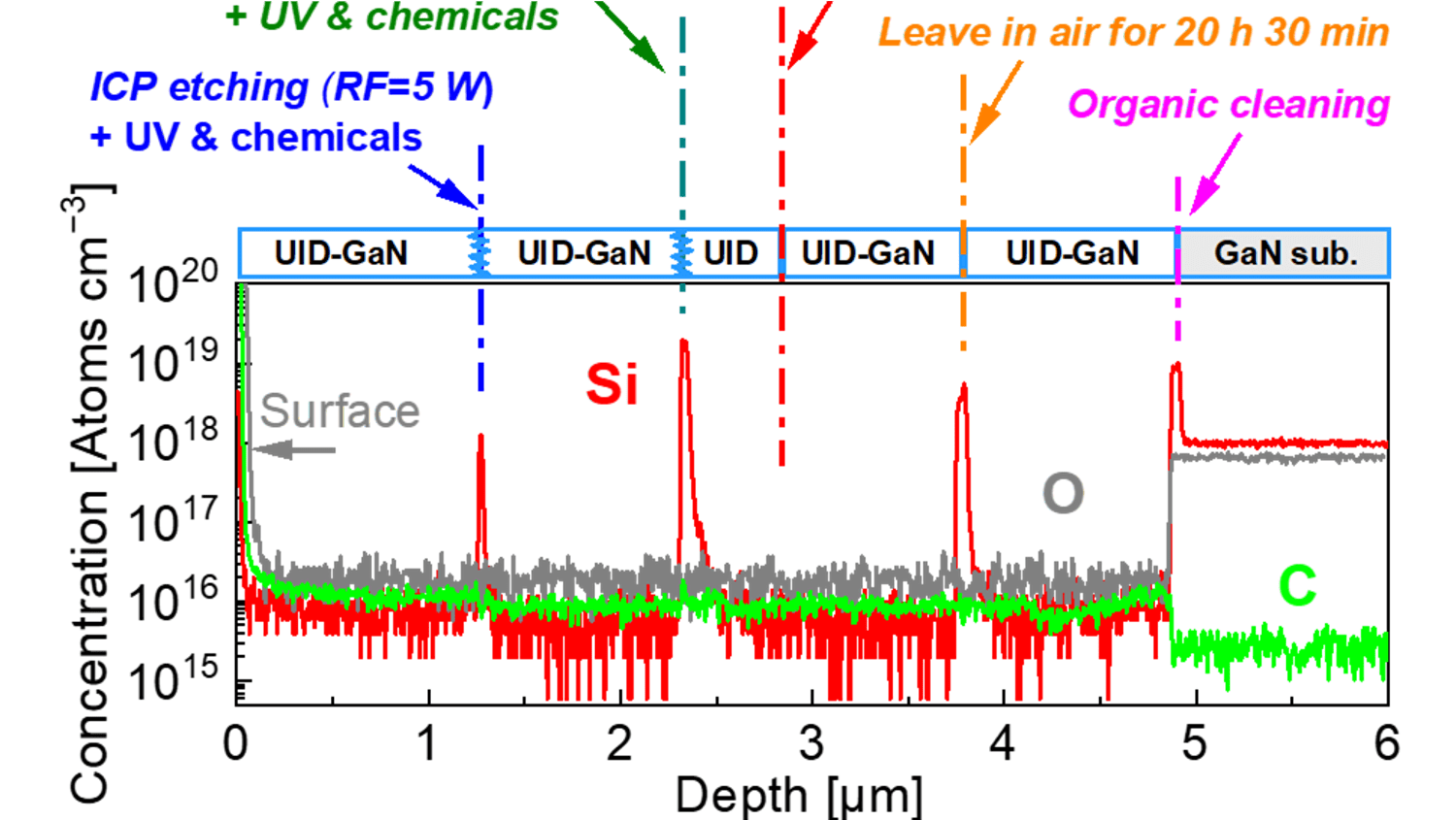
The development of gallium nitride (GaN) power devices requires a reliable selective-area doping process, which is difficult to achieve because of ongoing challenges associated with the required etch-then-regrow process. The presence of silicon (Si) impurities[…]
Chen’s Paper on Supercontinuum Generation Published in ACS Photonics!
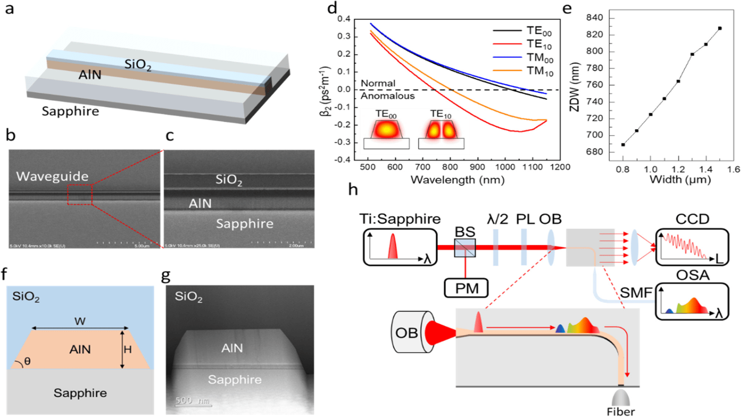
Optical sources emitting in the ultraviolet (UV) to near-infrared wavelength range are an enabling tools for a wide variety of applications. To achieve broadband coherent generation within visible and UV spectrum, one fundamental obstacle is[…]
Tsung-Han’s Paper on UWBG BN AlGaN/GaN MISHEMT Published in APL!
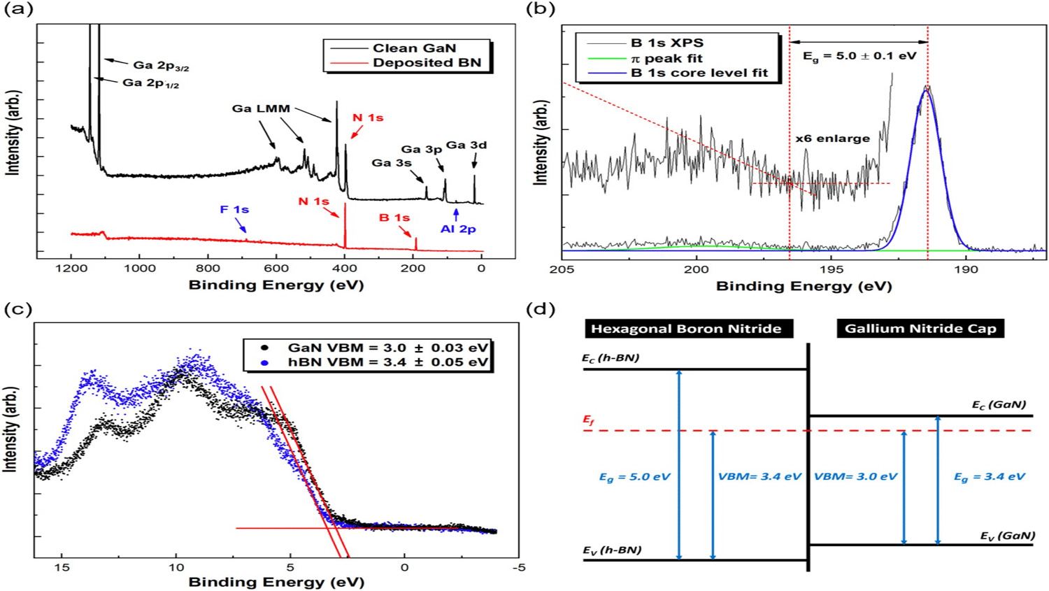
AlGaN/GaN metal–insulator–semiconductor high electron mobility transistors (MISHEMTs) were fabricated on Si substrates with a 10 nm boron nitride (BN) layer as a gate dielectric deposited by electron cyclotron resonance microwave plasma chemical vapor deposition. The material[…]


