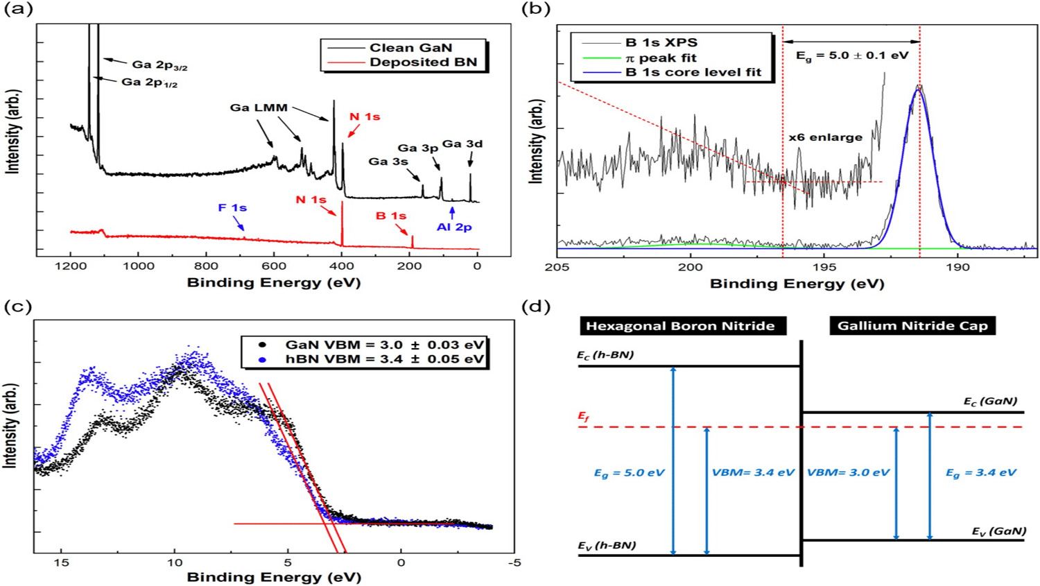
AlGaN/GaN metal–insulator–semiconductor high electron mobility transistors (MISHEMTs) were fabricated on Si substrates with a 10 nm boron nitride (BN) layer as a gate dielectric deposited by electron cyclotron resonance microwave plasma chemical vapor deposition. The material characterization of the BN/GaN interface was investigated by X-ray photoelectric spectroscopy (XPS) and UV photoelectron spectroscopy. The BN bandgap from the B1s XPS energy loss is ∼5 eV consistent with sp2 bonding. The MISHEMTs exhibit a low off-state current of 1 × 10⁻⁸ mA/mm, a high on/off current ratio of 109, a threshold voltage of −2.76 V, a maximum transconductance of 32 mS/mm at a gate voltage of −2.1 V and a drain voltage of 1 V, a subthreshold swing of 69.1 mV/dec, and an on-resistance of 12.75 Ω·mm. The interface state density (Dit) is estimated to be less than 8.49 × 1011 cm−2 eV−1. Gate leakage current mechanisms were investigated by temperature-dependent current–voltage measurements from 300 K to 500 K. The maximum breakdown electric field is no less than 8.4 MV/cm. Poole–Frenkel emission and Fowler–Nordheim tunneling are indicated as the dominant mechanisms of the gate leakage through the BN gate dielectric at low and high electric fields, respectively.