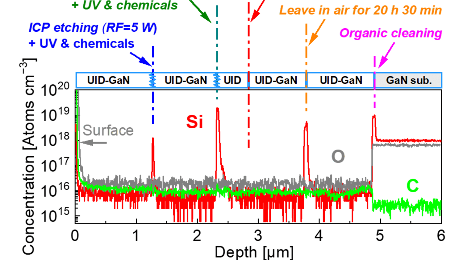
The development of gallium nitride (GaN) power devices requires a reliable selective-area doping process, which is difficult to achieve because of ongoing challenges associated with the required etch-then-regrow process. The presence of silicon (Si) impurities of unclear physical origin at the GaN regrowth interface has proven to be a major bottleneck. This paper investigates the origin of Si contamination at the epitaxial GaN-on-GaN interface, and demonstrates an approach that markedly reduces its impact on device performance. An optimized dry-etching approach combined with UV-ozone and chemical etching is shown to greatly reduce the Si concentration levels at the regrowth interface, and a significant improvement in reverse leakage current in vertical GaN-based p-n diodes is achieved.